High Accuracy Flip Chip Bonder M-1300
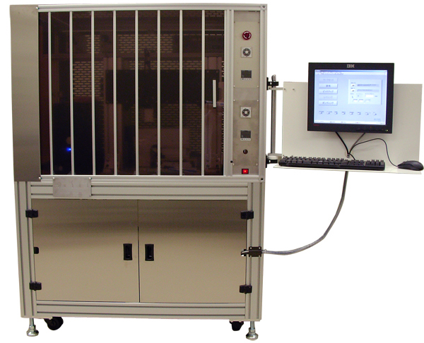
Ultra-high accuracy flip chip bonder with an alignment accuracy of ±1 micron
- This system is most suitable for laser-assisted packaging, optical device packaging and other ultra-high accuracy packaging applications.
- PC control provides high repeatability in terms of load, dispensing, heating and other conditions.
- This system allows bonding in an inert gas atmosphere and device orientation control based on laser displacement measurement.
- This system adopts the control method that realizes the highest-grade packaging accuracy among bonders of optical alignment type.
Features
- Ultra-high accuracy flip chip/die bonder developed for high-accuracy packaging of optical parts.
- Compatible with a wide variety of devices by changing the stage and collet parts.
- Adopts the optical alignment to recognize compound device edges and marks in glass parts.
- Allows chip bonding with a low concentration of oxygen (100 ppm or less), orientation control based on laser displacement measurement, high-accuracy packaging and chip bonding to 3D structures.
- Available with an extensive line-up of optional applications.
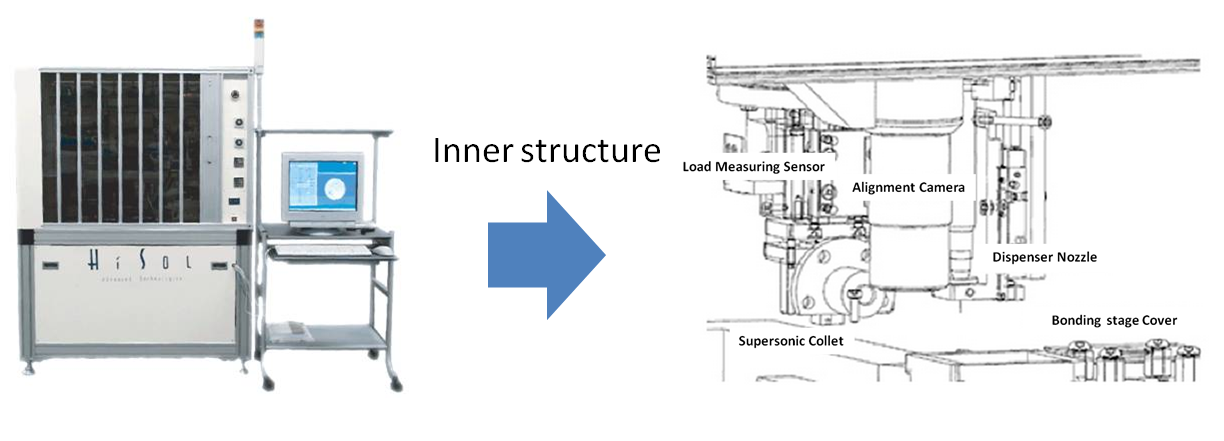
Compatibility of this system with various bonding methods
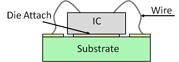
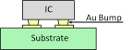
| Name of method | Eutectic die bonding |
Thermo-compression bonding |
Au soldering |
Anisotropic conductive paste (ACP) |
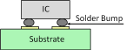
Solder bumping |
| Die bonding with eutectic metal | Bonding Au bumps and Au pads by heating and compression | Soldering Au bumps to pads | Bonding with anisotropic conductive paste (or film) | Bonding metal by soldering | |
 |
 |
 |
 |
 |
|
| Compatibility of this system | |||||
| Functions | Heating up to the eutectic material melting point | Heating and compression | Heating | Heating and compression | Heating |
| Temperature | Approx. 165°C to 400°C | 350-400℃ | 220-240℃ | 150-220℃ | 220-240℃ |
| Required pressure (I/O) | N/A | 80-100g | 2-10g | 50-100g | 5-10g |
| Ultrasonic effect | |||||
| Inert gas | Essential | Not required | Required | Not required | Required |
Data varies depending on materials used.
For details, refer to data provided by material manufacturers.
System specifications
| Model | M1300 |
|---|---|
| Function | Semi-automatic FC bonder |
| Alignment accuracy | ±1.0μm |
| Applied load | 50 to 5,000 g (load cell change) |
| Alignment | Manual for X- and Y-axes and automatic for θ-axis |
Equipment specifications
Optional parts
Pulse heater, ultrasonic bonding unit, inert gas bonding stage, alignment based on laser displacement measurement, etc.
Bonding stage for TO-15
(Chip handling tray shown on this side)
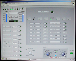
PC display for detailed bonding condition settings
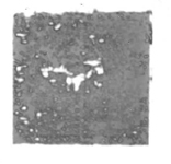
Void found in bonding with O2 of 1,000 ppm
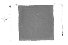
No void in bonding with O2 of 500 ppm